| CPC H04L 25/03057 (2013.01) [H01L 23/5227 (2013.01); H03F 3/189 (2013.01); H03M 1/12 (2013.01); H04L 25/03878 (2013.01)] | 20 Claims |

|
1. A semiconductor integrated circuit comprising:
a substrate including a first wiring layer and a second wiring layer, the second wiring layer separated from the first wiring layer in a stacking direction;
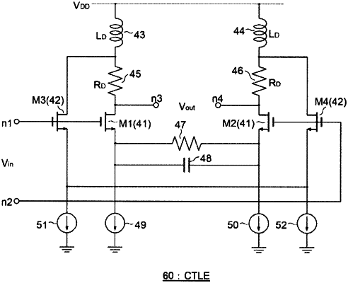
an equalization circuit disposed on the substrate and configured to amplify a signal level of a part of a frequency bandwidth included in a differential input signal, the differential input signal including a first signal and a second signal having logics opposite to each other, and configured to output a differential output signal including a third signal and a fourth signal, the third signal corresponding to the first signal and the fourth signal corresponding to the second signal;
a first node to which the first signal is input;
a second node to which the second signal is input;
a third node from which the third signal is output; and
a fourth node from which the fourth signal is output,
wherein the equalization circuit includes:
a first transistor having a gate connected to the first node and a drain connected to the third node,
a first inductor element and a first resistance element connected in series between the drain of the first transistor and a first reference voltage node,
a second transistor having a gate connected to the second node and a drain connected to the fourth node, and
a second inductor element and a second resistance element connected in series between the drain of the second transistor and the first reference voltage node,
wherein each of the first inductor element and the second inductor element is a part of a synthetic inductor element, the synthetic inductor element having a first inductor portion, a second inductor portion, and a third inductor portion,
the first inductor portion is disposed in a first region of the first wiring layer, has a first end portion, and includes a single-layer winding coil,
the second inductor portion is disposed in a second region of the first wiring layer, the second region being different from the first region, the second inductor portion has a second end portion, and includes a single-layer winding coil,
the third inductor portion is disposed at the second wiring layer, and has a third end portion and a fourth end portion, and
the third end portion of the third inductor portion is electrically connected to the first end portion of the first inductor portion, and the fourth end portion of the third inductor portion is electrically connected to the second end portion of the second inductor portion,
wherein the equalization circuit includes:
a third transistor having a gate connected to the first node, and a drain connected to a connection node of the first inductor element and the first resistance element, and
a fourth transistor having a gate connected to the second node, and a drain connected to a connection node of the second inductor element and the second resistance element.
|