| CPC H03K 19/0016 (2013.01) [G11C 5/148 (2013.01); H03K 17/693 (2013.01); G11C 2207/2227 (2013.01); H03K 2217/0081 (2013.01)] | 9 Claims |

|
1. A semiconductor device comprising:
a memory block; and
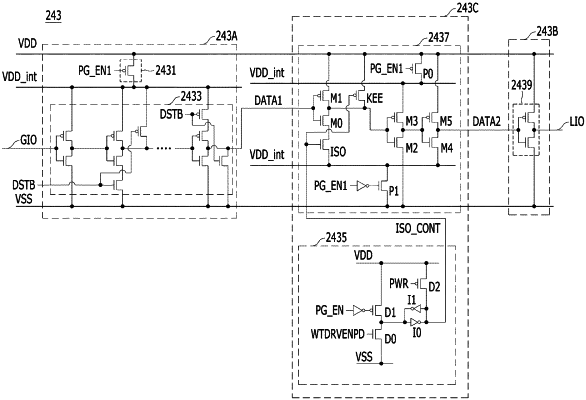
a write driving block having first and second power gating structures different from each other, and suitable for transmitting a data signal to the memory block by using at least third and fourth voltages supplied from the first and second power gating structures during an operation period according to a write mode and fixing an input terminal of the memory block to a set voltage level by using one of first and second voltages during a particular period according to a power-down mode,
wherein each of the first and second power gating structures is coupled to at least one of a supply terminal of the first voltage and a supply terminal of the second voltage, and cuts off the supply of at least one of the first voltage and the second voltage in the power-down mode,
wherein the write driving block includes:
a first circuit having the first power gating structure, and suitable for generating, during the operation period, a first write data signal through an output terminal, which corresponds to the data signal, based on a data strobe signal, the output terminal of the first circuit being floated during the particular period;
a second circuit suitable for transmitting a second write data signal to the input terminal of the memory block during the operation period and fixing the input terminal of the memory block to the first voltage level during the particular period; and
a third circuit having the second power gating structure, and suitable for generating the second write data signal, which corresponds to the first write data signal, during the operation period, and fixing an input of the second circuit to a second voltage level regardless of the floated output terminal of the first circuit during the particular period.
|