| CPC H01S 5/18 (2013.01) [H01S 5/0206 (2013.01); H01S 5/11 (2021.01); H01S 5/2081 (2013.01); H01S 5/34333 (2013.01); H01S 2304/04 (2013.01)] | 7 Claims |

|
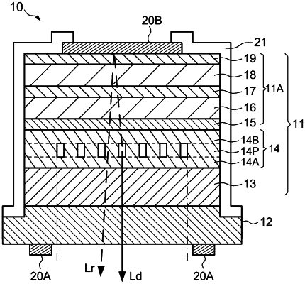
1. A manufacturing method for manufacturing a surface-emitting laser device made of a GaN-based semiconductor by an MOVPE method, the manufacturing method comprising steps of:
(a) growing a first cladding layer of a first conductive type on a substrate, with a {0001} plane as a growth plane;
(b) growing a guide layer on the first cladding layer;
(c) forming holes in a surface of the guide layer by etching, the holes being two-dimensionally periodically arranged within a plane parallel to the guide layer;
(d) etching the guide layer by using an etchant having selectivity to a {10−10} plane of the guide layer;
(e) supplying a gas containing a nitrogen source to cause mass transport without supplying a group-III material gas, and then supplying the group-III material gas for growth, whereby a first embedding layer closing openings of the holes is formed to form a photonic crystal layer; and
(f) growing an active layer and a second cladding layer of a second conductive type in this order on the first embedding layer, the second conductive type being opposite to the first conductive type, wherein
in the steps (e) and (f), air holes formed in the photonic crystal layer have a hexagonal column shape surrounded by the {10−10} planes, and the air holes have a diameter distribution including a single unimodal distribution with a standard deviation (α) of 1 nm or less, and a proportion of air holes belonging to the unimodal distribution to all the air holes is 95% or higher.
|