| CPC H01M 4/625 (2013.01) [H01M 4/1391 (2013.01); H01M 4/1393 (2013.01); H01M 4/364 (2013.01); H01M 4/621 (2013.01); H01M 10/0525 (2013.01); G06V 10/50 (2022.01)] | 9 Claims |

|
1. A secondary battery electrode comprising a mixture layer containing graphene and a secondary battery active material,
wherein the mixture layer comprises conductive material portions in a cross section of the secondary battery electrode, the conductive material portions having an average aspect ratio of 2.0 or more and 3.0 or less, the aspect ratio of the conductive material portions being determined by a method described below;
wherein the method of determining the average aspect ratio of the conductive material portions comprises:
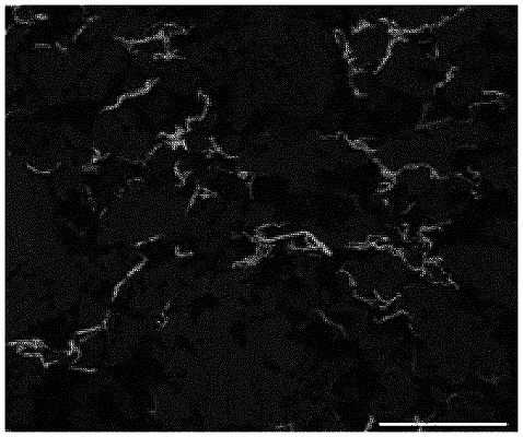
(1) acquiring a mapping image and a histogram of spreading resistance values of a mixture layer portion by scanning spreading resistance microscopy;
(2) defining a lowest resistance value in the histogram as R1, sequentially accumulating frequency from R1, defining a spreading resistance value when a cumulative frequency exceeds 3% of a cumulative frequency of entire data as R2, further defining a spreading resistance value that is 10 times R2 as R3, binarizing the mapping image with R3 as a threshold, and defining portions having a resistance value equal to or less than R3 as the conductive material portions; and
(3) performing image analysis of the binarized mapping image to determine the average aspect ratio of the conductive material portions.
|