US 11,837,670 B2
Semiconductor devices with single-photon avalanche diodes, light scattering structures, and multiple deep trench isolation structures
Marc Allen Sulfridge, Boise, ID (US); Anne Deignan, County Limerick (IE); Nader Jedidi, Cork (IE); and Michael Gerard Keyes, Dromcollogher (IE)
Assigned to SEMICONDUCTOR COMPONENTS INDUSTRIES, LLC, Scottsdale, AZ (US)
Filed by SEMICONDUCTOR COMPONENTS INDUSTRIES, LLC, Phoenix, AZ (US)
Filed on Oct. 21, 2020, as Appl. No. 16/949,228.
Claims priority of provisional application 62/981,902, filed on Feb. 26, 2020.
Claims priority of provisional application 62/943,475, filed on Dec. 4, 2019.
Prior Publication US 2021/0175265 A1, Jun. 10, 2021
Int. Cl. H01L 31/02 (2006.01); H04N 25/63 (2023.01); H01L 27/146 (2006.01); H01L 31/055 (2014.01); H01L 31/107 (2006.01); H01L 31/0232 (2014.01); G02B 3/06 (2006.01)
CPC H01L 31/02027 (2013.01) [G02B 3/06 (2013.01); H01L 27/1463 (2013.01); H01L 27/14605 (2013.01); H01L 27/14621 (2013.01); H01L 27/14627 (2013.01); H01L 27/14629 (2013.01); H01L 27/14643 (2013.01); H01L 27/14649 (2013.01); H01L 31/02327 (2013.01); H01L 31/055 (2013.01); H01L 31/107 (2013.01); H01L 27/1464 (2013.01); H04N 25/63 (2023.01)] 20 Claims
OG exemplary drawing
 
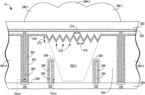
1. A semiconductor device comprising:
a substrate having a thickness;
a single-photon avalanche diode in the substrate;
a first deep trench isolation structure in the substrate that forms a first ring around the single-photon avalanche diode; and
a second deep trench isolation structure in the substrate that forms a second ring around the single-photon avalanche diode, wherein the second deep trench isolation structure has a depth that is less than the thickness.