| CPC H01L 29/7813 (2013.01) [H01L 29/1608 (2013.01); H01L 29/66727 (2013.01); H01L 29/66734 (2013.01)] | 23 Claims |

|
1. A power semiconductor device comprising:
a semiconductor layer structure comprising a drift region that comprises a wide band-gap semiconductor material having a first conductivity type;
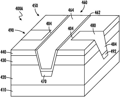
a plurality of gate trenches in an upper portion of the semiconductor layer structure, each gate trench having a longitudinal axis that extends in a first direction and comprising first and second opposed sidewalls that each extend in the first direction;
a plurality of source trenches in an upper portion of the semiconductor layer structure, each source trench having a longitudinal axis that extends in a second direction that is different from the first direction and comprising first and second opposed sidewalls that each extend in the second direction; and
a plurality of deep shielding regions having the second conductivity type in the semiconductor layer structure underneath the respective source trenches.
|