| CPC H01L 29/7397 (2013.01) [H02M 1/08 (2013.01); H02M 3/003 (2021.05); H02M 7/003 (2013.01); H02M 7/5387 (2013.01); H03K 17/168 (2013.01); H02M 1/0054 (2021.05)] | 20 Claims |

|
1. A method for controlling a semiconductor device, the semiconductor device including:
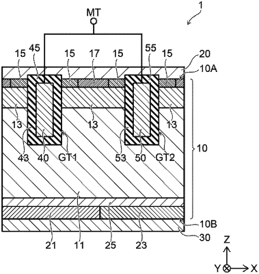
a semiconductor part provided between a first electrode and a second electrode;
at least a control electrode being provided between the semiconductor part and the first electrode;
a first insulating film provided between the semiconductor part and the control electrode; and
a second insulating film provided between the first electrode and the control electrode;
the semiconductor part including first to fifth semiconductor layers, the first, third and fifth semiconductor layers being of a first conductivity type, the second and fourth semiconductor layers being of a second conductivity type,
the second semiconductor layer being provided between the first semiconductor layer and the first electrode, the second semiconductor layer including a portion facing the control electrode via the first insulating film,
the third semiconductor layer being provided between the second semiconductor layer and the first electrode, the third semiconductor layer contacting the first insulating film,
the fourth semiconductor layer being provided between the first semiconductor layer and the second electrode,
the fifth semiconductor layer being provided between the first semiconductor layer and the second electrode, the fourth and fifth semiconductor layers being arranged along the second electrode,
the first electrode being electrically connected to the second and third semiconductor layers,
the second electrode being electrically connected to the fourth and fifth semiconductor layers,
the method comprising:
applying a first control voltage between the first electrode and the control electrode in a first period;
applying a second control voltage between the first electrode and the control electrode in a second period after the first period, the second control voltage being greater than the first control voltage; and
applying a third control voltage between the first electrode and the control electrode in a third period after the second period, the third control voltage being greater than the first control voltage and less than the second control voltage.
|