| CPC H01L 29/6681 (2013.01) [H01L 21/02282 (2013.01); H01L 21/76224 (2013.01); H01L 21/76229 (2013.01); H01L 21/76837 (2013.01); H01L 21/823431 (2013.01); H01L 21/823481 (2013.01); H01L 21/823821 (2013.01); H01L 21/823878 (2013.01); H01L 27/0924 (2013.01); H01L 29/0649 (2013.01); H01L 29/0653 (2013.01); H01L 29/0847 (2013.01); H01L 29/42392 (2013.01); H01L 29/78696 (2013.01); H10B 10/12 (2023.02); H10B 10/18 (2023.02); H01L 29/0673 (2013.01)] | 20 Claims |

|
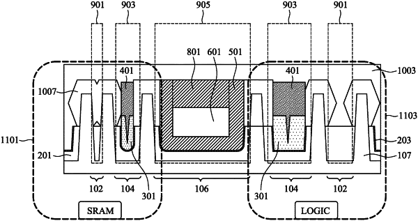
1. A semiconductor device comprising:
a plurality of semiconductor fins over a substrate;
an isolation layer covering a bottom portion of the plurality of semiconductor fins;
a blocking layer covering at least a portion of the isolation layer;
an insulation fin structure located at least partially over the blocking layer and between a first one of the plurality of semiconductor fins and a second one of the plurality of semiconductor fins, wherein the insulation fin structure comprises a bottom portion made of a conformal nitride material and a seamless top portion made of an oxide material, wherein the seamless top portion covers a top surface of the conformal nitride material, and wherein the seamless top portion comprises tungsten oxide;
a shallow trench isolation located on an opposite side of the first one of the plurality of semiconductor fins from the insulation fin structure, the shallow trench isolation comprising a first material free from overlying portions of the nitride material and free from overlying portions of the oxide material;
an SRAM source/drain region in physical contact with the insulation fin structure;
a second insulation fin structure in physical contact with the SRAM source/drain region, the second insulative fin comprising:
a first dielectric material, the isolation layer comprising the first dielectric material;
a second dielectric material over the first dielectric material, the second dielectric material being different from the first dielectric material;
a third dielectric material embedded within the second dielectric material, the third dielectric material being different from the second dielectric material; and
a fourth dielectric material overlying the third dielectric material, the fourth dielectric material being different from the third dielectric material; and
a logic device located on an opposite side of the second insulation fin from the SRAM source/drain region, a portion of the logic device being in physical contact with the second insulative fin.
|
|
10. A semiconductor device comprising:
a first source/drain region in physical contact with an insulative fin, the insulative fin comprising:
a first dielectric material adjacent to a semiconductor substrate;
a second dielectric material over the first dielectric material, the second dielectric material being different from the first dielectric material, the second dielectric material being conformal to the first dielectric material; and
a third dielectric material, wherein the third dielectric material is free from seams and voids, wherein the first source/drain region is in physical contact with the third dielectric material;
a second source/drain region in physical contact with the insulative fin, the second source/drain region being located on an opposite side of the insulative fin from the first source/drain region, wherein the first source/drain region is part of a static random access memory device;
a second insulative fin in physical contact with the second source/drain region, the second insulative fin comprising:
the first dielectric material;
a fourth dielectric material over the first dielectric material, the fourth dielectric material being different from the first dielectric material;
a fifth dielectric material embedded within the fourth dielectric material, the fifth dielectric material being different from the fourth dielectric material; and
a sixth dielectric material overlying the fifth dielectric material, the sixth dielectric material being different from the fifth dielectric material; and
a logic device located on an opposite side of the second insulative fin from the static random access memory device, a portion of the logic device being in physical contact with the second insulative fin.
|
|
14. A semiconductor device comprising:
a first fin and a second fin over a semiconductor substrate, a first region being located between the first fin and the second fin; and
a dielectric fin located within the first region, the dielectric fin comprising:
a first dielectric material;
a second dielectric material overlying the first dielectric material, the second dielectric material being different from the first dielectric material, wherein the second dielectric material comprises silicon nitride;
a third dielectric material overlying and in direct physical contact with the second dielectric material, the third dielectric material being different from the second dielectric material, the third dielectric material being free from seams and voids, wherein external sidewalls of the third dielectric material are aligned with external sidewalls of the second dielectric material;
a fourth dielectric material in physical contact with both a top surface of the third dielectric material and a sidewall of the third dielectric material, the sidewall being at a right angle to the top surface;
a blocking layer between the first dielectric layer and the second dielectric layer; and
an SRAM source/drain region in physical contact with the dielectric fin;
a second dielectric fin in physical contact with the SRAM source/drain region, the second dielectric fin comprising:
the first dielectric material;
a fifth dielectric material over the first dielectric material, the fifth dielectric material being different from the first dielectric material;
a sixth dielectric material embedded within the fifth dielectric material, the sixth dielectric material being different from the fifth dielectric material; and
a seventh dielectric material overlying the sixth dielectric material, the seventh dielectric material being different from the sixth dielectric material; and
a logic device located on an opposite side of the second dielectric fin from the SRAM source/drain region, a portion of the logic device being in physical contact with the second dielectric fin.
|