| CPC H01L 29/45 (2013.01) [H01L 21/28518 (2013.01); H01L 21/76805 (2013.01); H01L 21/76843 (2013.01); H01L 21/76859 (2013.01); H01L 21/76886 (2013.01); H01L 21/823431 (2013.01); H01L 23/485 (2013.01); H01L 23/5226 (2013.01); H01L 23/53266 (2013.01); H01L 29/0673 (2013.01); H01L 29/0847 (2013.01); H01L 29/41766 (2013.01); H01L 29/41791 (2013.01); H01L 29/42392 (2013.01); H01L 29/456 (2013.01); H01L 29/66795 (2013.01); H01L 29/775 (2013.01); H01L 29/7851 (2013.01); H01L 29/78696 (2013.01)] | 20 Claims |

|
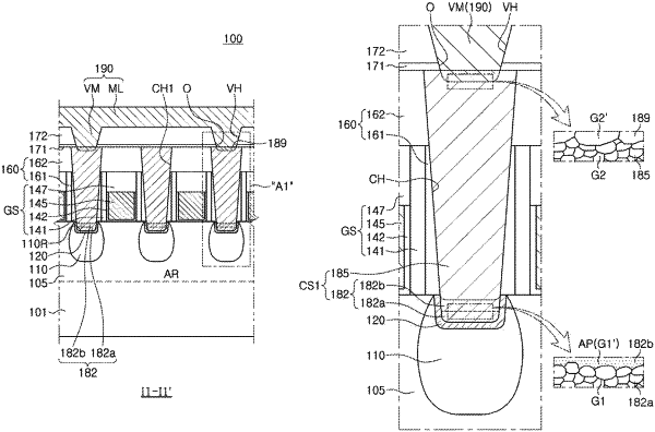
1. A method of manufacturing a semiconductor device, the method comprising:
forming a gate structure and a source/drain region on a fin active region at least one side of the gate structure on a substrate;
forming an insulating structure covering the fin active region, the gate structure, and the source/drain region;
forming a contact hole exposing a portion of the source/drain region through the insulating structure;
forming a seed layer having a first grain size on an exposed portion of the source/drain region;
applying an ion implantation process to the seed layer such that an upper region of the seed layer is amorphous or has a grain size different from the first grain size, and a lower region of the seed layer has the first grain size; and,
forming a contact plug having a second grain size on the seed layer within the contact hole.
|