| CPC H01L 29/42316 (2013.01) [H01L 21/022 (2013.01); H01L 21/0217 (2013.01); H01L 21/02164 (2013.01); H01L 21/02178 (2013.01); H01L 21/28587 (2013.01); H01L 21/765 (2013.01); H01L 23/3171 (2013.01); H01L 23/3192 (2013.01); H01L 29/2003 (2013.01); H01L 29/205 (2013.01); H01L 29/404 (2013.01); H01L 29/66462 (2013.01); H01L 29/7786 (2013.01)] | 35 Claims |

|
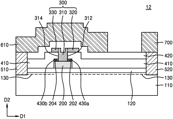
1. A semiconductor device comprising:
a channel layer including a channel;
a channel supply layer on the channel layer, an interface between the channel supply layer and the channel layer being adjacent to the channel;
a channel separation pattern on the channel supply layer;
a gate electrode pattern on the channel separation pattern, a size of the gate electrode pattern in a first direction being different from a size of the channel separation pattern in the first direction, the first direction being parallel with an upper surface of the channel layer;
an electric-field relaxation pattern protruding from a first lateral surface of the gate electrode pattern in the first direction;
a first passivation film between the electric-field relaxation pattern and the channel supply layer;
a first passivation pattern between the first passivation film and the channel separation pattern, the first passivation pattern on the first lateral surface of the gate electrode pattern; and
a second passivation pattern between the first passivation film and the channel separation pattern, the second passivation pattern on a second lateral surface of the gate electrode pattern, wherein
the electric-field relaxation pattern and gate electrode pattern forming a single structure,
a lateral surface of the first passivation pattern and a lateral surface of the channel separation pattern are coplanar and immediately adjacent to each other, and
a lateral surface of the second passivation pattern and an other lateral surface of the channel separation pattern are coplanar and immediately adjacent to each other.
|