US 11,837,641 B2
Gate-all-around integrated circuit structures having adjacent deep via substrate contacts for sub-fin electrical contact
Biswajeet Guha, Hillsboro, OR (US); William Hsu, Hillsboro, OR (US); Chung-Hsun Lin, Portland, OR (US); Kinyip Phoa, Beaverton, OR (US); Oleg Golonzka, Beaverton, OR (US); Tahir Ghani, Portland, OR (US); Kalyan Kolluru, Portland, OR (US); Nathan Jack, Forest Grove, OR (US); Nicholas Thomson, Hillsboro, OR (US); Ayan Kar, Portland, OR (US); and Benjamin Orr, Munich (DE)
Assigned to Intel Corporation, Santa Clara, CA (US)
Filed by Intel Corporation, Santa Clara, CA (US)
Filed on Dec. 18, 2019, as Appl. No. 16/719,281.
Prior Publication US 2021/0193807 A1, Jun. 24, 2021
Int. Cl. H01L 29/41 (2006.01); H01L 29/417 (2006.01); H01L 25/18 (2023.01); H01L 27/088 (2006.01); H01L 29/06 (2006.01); H01L 29/40 (2006.01); H01L 29/423 (2006.01); H01L 29/66 (2006.01); H01L 29/78 (2006.01)
CPC H01L 29/41791 (2013.01) [H01L 25/18 (2013.01); H01L 27/0886 (2013.01); H01L 29/0673 (2013.01); H01L 29/401 (2013.01); H01L 29/42392 (2013.01); H01L 29/6653 (2013.01); H01L 29/6681 (2013.01); H01L 29/7853 (2013.01); H01L 2029/7858 (2013.01)] 18 Claims
OG exemplary drawing
 
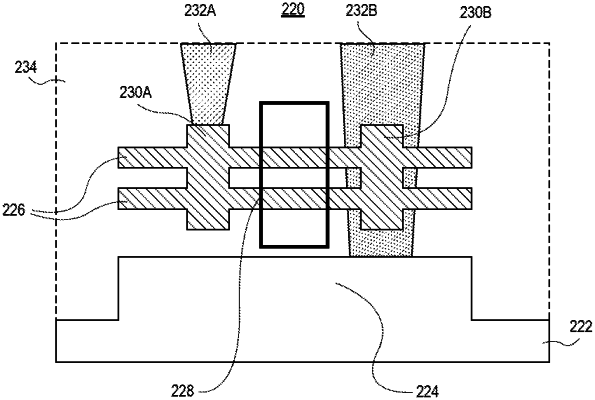
1. An integrated circuit structure, comprising: a conductive via above a semiconductor substrate, the conductive via comprising a metal-containing material; a vertical arrangement of horizontal nanowires above a fin protruding from the semiconductor substrate, a channel region of the vertical arrangement of horizontal nanowires electrically isolated from the fin, wherein the fin is in direct contact with the metal-containing material of the conductive via; and a gate stack over the vertical arrangement of horizontal nanowires.