| CPC H01L 27/14636 (2013.01) [H01L 27/14641 (2013.01)] | 5 Claims |

|
1. A photo receiver comprising:
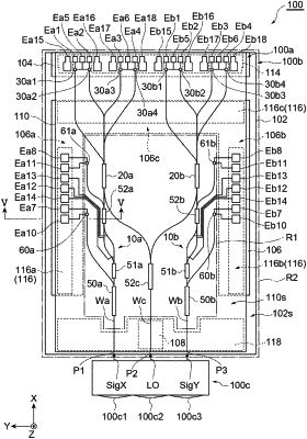
a photo detector including a semiconductor substrate having a first main surface and a second main surface opposite to the first main surface, and a metal pattern layer provided on the second main surface; and
a carrier including a supporting substrate having a third main surface facing the second main surface, and a solder pattern layer provided on the third main surface, the solder pattern layer being bonded to the metal pattern layer,
the first main surface being provided with a variable optical attenuator, an optical 90-degree hybrid device, and a plurality of photodiodes optically coupled to the variable optical attenuator via the optical 90-degree hybrid device, and
the solder pattern layer and the metal pattern layer being located in a peripheral area surrounding a central area where the variable optical attenuator and the optical 90-degree hybrid device are located when viewed in a normal direction of the first main surface,
whereby the solder pattern layer and the metal pattern layer are not located in the central area when viewed in the normal direction of the first main surface.
|