| CPC H01L 27/124 (2013.01) [G09G 3/20 (2013.01); G09G 2300/0426 (2013.01); G09G 2310/08 (2013.01); G09G 2330/12 (2013.01)] | 11 Claims |

|
1. An array substrate, comprising:
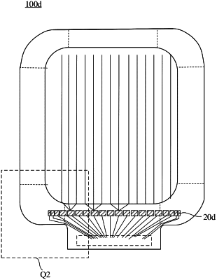
a substrate having a display region and a non-display region surrounding the display region, the non-display region comprising a first sub-region extending in a first direction, a second sub-region extending in a second direction intersecting with the first direction, and a third sub-region connecting the first sub-region with the second sub-region, and the third sub-region extending in an arc shape, and the first sub-region comprising a binding region;
a plurality of signal lines extending in the display region, each of the signal lines extending along the second direction;
a plurality of circuit modules located on the substrate, wherein at least part of the circuit modules are located between the display region and the binding region, each of the circuit modules is electrically connected to at least two of the signal lines, a part of the circuit modules are arranged in the first sub-region along the first direction, and another part of the circuit modules are arranged in an array in the third sub-region along an arc-shaped extending direction of the third sub-region;
a plurality of fan-out lines located in the non-display region, wherein each of the fan-out lines is electrically connected to a corresponding one of the circuit modules and extends to the binding region, and
a plurality of control lines configured to control conductions between the fan-out lines and corresponding signal lines, wherein:
each of the circuit modules comprises a demultiplexer, the demultiplexer comprises two or more first transistors, each of the first transistors comprises a first gate, a first electrode and a second electrode, and in the demultiplexer, the first gates of the first transistors are respectively electrically connected to the control lines, the first electrodes of the first transistors are respectively electrically connected to the corresponding signal lines, and the second electrodes of the first transistors extend to the binding region through a same fan-out line, and/or
each of the circuit modules comprises a detection module, the detection module comprises two or more second transistors, each of the second transistors comprises a second gate, a third electrode and a fourth electrode, and in the detection module, the second gates of the second transistors are respectively electrically connected to the control lines, the third electrodes of the second transistors are respectively electrically connected to the corresponding signal lines of a same signal type, and the fourth electrodes of the second transistors extend to the binding region through the fan-out line.
|