| CPC H01L 25/0753 (2013.01) [H01L 27/1214 (2013.01); H01L 33/62 (2013.01); H01L 2223/6633 (2013.01); H01L 2933/0066 (2013.01)] | 21 Claims |

|
1. A display device comprising:
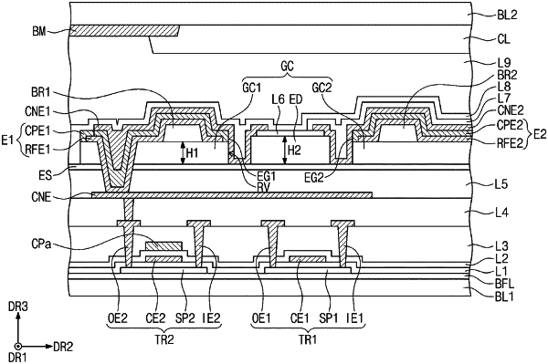
a first wall structure disposed on a substrate;
a second wall structure disposed on the substrate and spaced apart from the first wall structure;
a first electrode disposed on the first wall structure;
a second electrode disposed on the second wall structure and spaced apart from the first electrode;
a light emitting element disposed between the first wall structure and the second wall structure, the light emitting element electrically connected with the first electrode and the second electrode;
a first insulating layer disposed between the substrate and the light emitting element;
a first connection electrode disposed on the first electrode and directly contacting with a first end portion of the light emitting element, and
a second connection electrode disposed on the second electrode and directly contacting with a second end portion of the light emitting element, wherein
the first wall structure comprises a first guide layer disposed on the substrate and a first wall directly disposed on the first guide layer.
|