US 11,837,582 B2
Molded direct bonded and interconnected stack
Guilian Gao, Campbell, CA (US); Cyprian Emeka Uzoh, San Jose, CA (US); Jeremy Alfred Theil, Mountain View, CA (US); Belgacem Haba, Saratoga, CA (US); and Rajesh Katkar, Milpitas, CA (US)
Assigned to ADEIA SEMICONDUCTOR BONDING TECHNOLOGIES INC., San Jose, CA (US)
Filed by ADEIA SEMICONDUCTOR BONDING TECHNOLOGIES INC., San Jose, CA (US)
Filed on Dec. 29, 2022, as Appl. No. 18/148,327.
Application 18/148,327 is a continuation of application No. 17/448,794, filed on Sep. 24, 2021, granted, now 11,764,189.
Application 17/448,794 is a continuation of application No. 16/460,068, filed on Jul. 2, 2019, granted, now 11,158,606, issued on Oct. 26, 2021.
Claims priority of provisional application 62/694,845, filed on Jul. 6, 2018.
Prior Publication US 2023/0253367 A1, Aug. 10, 2023
This patent is subject to a terminal disclaimer.
Int. Cl. H01L 25/065 (2023.01); H01L 21/768 (2006.01); H01L 23/538 (2006.01); H01L 23/00 (2006.01)
CPC H01L 25/0657 (2013.01) [H01L 21/76898 (2013.01); H01L 23/5384 (2013.01); H01L 23/5385 (2013.01); H01L 23/5386 (2013.01); H01L 24/95 (2013.01)] 33 Claims
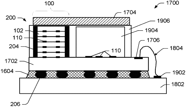
OG exemplary drawing
 
1. A microelectronic assembly comprising:
a substrate;
a first die and a first bonding layer on the first die, the first bonding layer directly bonded to the substrate without an adhesive;
a second die having a microelectronic circuit element formed therein and disposed over the first die, the first die directly bonded to a second bonding layer on the second die without an adhesive;
a first encapsulating layer disposed adjacent a side wall of the second die; and
a second encapsulating layer deposited on and laterally adjacent the first encapsulating layer, the second encapsulating layer comprising an inorganic material.