| CPC H01L 24/75 (2013.01) [H01L 2224/75252 (2013.01); H01L 2224/75303 (2013.01); H01L 2224/75502 (2013.01); H01L 2924/3511 (2013.01)] | 12 Claims |

|
1. A chip bonding apparatus, comprising:
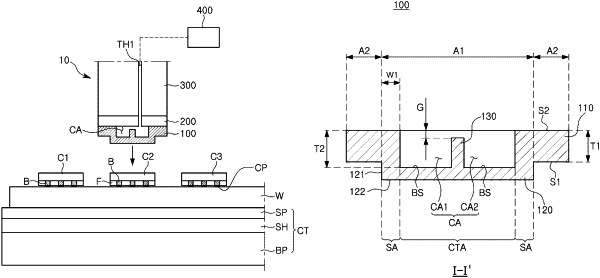
a bonding contact configured to apply a bonding force to a semiconductor chip disposed on a substrate, the bonding contact having a first surface configured to face the semiconductor chip and a second surface opposite the first surface, the bonding contact including a protruding portion on the first surface, the protruding portion configured to contact the semiconductor chip, the bonding contact including a cavity formed in a region vertically overlapping the protruding portion;
a heater disposed to be in contact with the second surface of the bonding contact to cover the cavity, and configured to heat the bonding contact;
a bonding head disposed above the heater and configured to transmit the bonding force; and
a partition wall structure protruding from a bottom surface of the cavity to partition an inner space of the cavity,
wherein an upper surface of the partition wall structure is at a lower level than that of the second surface of the bonding contact,
wherein the cavity has a depth of 0.5 mm to 1.5 mm, and
the partition wall structure is at a level of 0.2 mm to 0.5 mm lower than the second surface of the bonding contact.
|