| CPC H01L 23/5329 (2013.01) [H01L 21/768 (2013.01); H01L 27/0207 (2013.01); H10B 12/033 (2023.02); H10B 12/053 (2023.02); H10B 12/315 (2023.02); H10B 12/34 (2023.02); H10B 12/482 (2023.02); H10B 12/485 (2023.02); H01L 21/7682 (2013.01); H01L 21/76897 (2013.01); H01L 23/5222 (2013.01)] | 20 Claims |

|
1. A semiconductor memory device comprising:
a substrate;
a device isolation layer disposed in the substrate defining an active region extending in a first direction;
first conductive lines disposed in the active region and extending in a second direction crossing the first direction;
a second conductive line disposed on the active region between the first conductive lines and extending in a third direction crossing the first direction and the second direction;
an insulating pattern disposed on the second conductive line;
a bit line node contact disposed between the active region and the second conductive line;
a landing pad disposed on an edge portion of the active region;
a storage node contact between the landing pad and the edge portion of the active region;
a buried pattern disposed between the bit line node contact and the storage node contact;
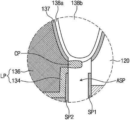
a first spacer disposed between a sidewall of the second conductive line and the landing pad;
an air spacer disposed between the first spacer and the landing pad; and
a capping pattern protruding from a sidewall of the landing pad and disposed on the air spacer,
wherein the capping pattern is spaced apart from the first spacer, and
wherein the air spacer is in contact with a sidewall of the insulating pattern.
|