| CPC H01L 23/5226 (2013.01) [H01L 23/3157 (2013.01); H01L 23/49531 (2013.01); H01L 23/49534 (2013.01); H01L 23/5283 (2013.01); H01L 24/09 (2013.01); H01L 2224/02372 (2013.01); H01L 2224/02377 (2013.01); H01L 2224/02379 (2013.01); H01L 2924/3511 (2013.01)] | 20 Claims |

|
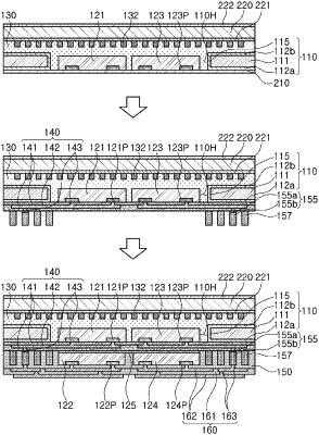
1. A fan-out semiconductor package comprising:
a connection structure including a redistribution layer containing a signal pattern;
a first semiconductor chip disposed on the connection structure, the first semiconductor chip having a first active surface on which a first connection pad is disposed and a first inactive surface opposing the first active surface;
first metal members disposed on the connection structure and electrically connected to the signal pattern;
second metal members disposed on the connection structure and electrically insulated from the signal pattern and the first semiconductor chip; and
an encapsulant disposed on the connection structure and respectively covering at least portions of the first semiconductor chip and the first and second metal members,
wherein the first connection pad is electrically connected to the first metal members through the signal pattern of the redistribution layer, and
wherein an entire lower surface of each of the second metal members is covered by the encapsulant.
|