| CPC H01L 23/49816 (2013.01) [H01L 23/3185 (2013.01); H01L 23/5383 (2013.01); H01L 23/5385 (2013.01); H01L 23/5389 (2013.01); H01L 25/18 (2013.01)] | 20 Claims |

|
1. A semiconductor package comprising:
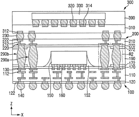
a first substrate including a first surface including a first region and a second region at least partially surrounding the first region, wherein the first substrate includes a first insulating layer, a first conductive pattern in the first insulating layer, a first passivation layer disposed in the first region and the second region, and a second passivation layer disposed on the first passivation layer in the second region;
an interposer overlapping the first substrate and including a second insulating layer and a second conductive pattern in the second insulating layer;
a first connection terminal disposed on the first passivation layer in the first region; and
a second connection terminal disposed on the second passivation layer in the second region,
wherein the first conductive pattern and the second conductive pattern are connected to each other through the first connection terminal and the second connection terminal,
wherein the first connection terminal and the second connection terminal do not overlap vertically, and
wherein the first connection terminal and the second connection terminal are disposed at a same vertical level as each other, wherein the first connection terminal contacts the first passivation layer and does not contact the second passivation laver, wherein the second connection terminal contacts the first passivation layer and the second passivation layer.
|