| CPC H01L 23/3121 (2013.01) [H01F 27/36 (2013.01); H01F 27/363 (2020.08); H01F 38/14 (2013.01); H01L 21/32051 (2013.01); H01L 23/10 (2013.01); H01L 23/49822 (2013.01); H01L 23/5227 (2013.01); H01L 23/5389 (2013.01); H01L 23/645 (2013.01); H02J 7/0042 (2013.01); H02J 50/10 (2016.02); H04B 5/0037 (2013.01); H04B 5/0075 (2013.01); H01L 2224/04105 (2013.01); H01L 2224/19 (2013.01); H01L 2224/73267 (2013.01); H01L 2924/19042 (2013.01); H01L 2924/19105 (2013.01)] | 20 Claims |

|
1. A semiconductor device package, comprising:
a semiconductor device;
a molding material surrounding the semiconductor device; and
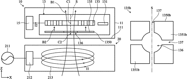
a conductive slot positioned over the molding material and having an opening and at least two channels connecting the opening to the edges of the conductive slot, and at least two of the channels extend in different directions, wherein the conductive slot is divided by the channels as a plurality of sub-portions, and one of the sub-portions has a first edge, a second edge, and a third edge that extend in different directions.
|