| CPC H01L 22/34 (2013.01) [H01L 22/32 (2013.01); H01L 23/5226 (2013.01); H01L 23/5228 (2013.01)] | 20 Claims |

|
1. A semiconductor device, comprising:
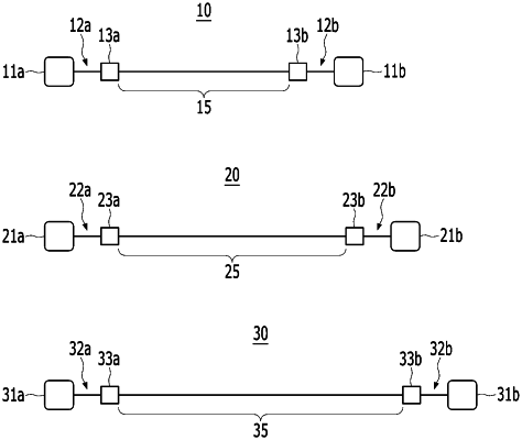
a first resistance chain including first upper resistance segments, first resistance via plugs, and first lower resistance segments;
a second resistance chain including second upper resistance segments, second resistance via plugs, and second lower resistance segments; and
a third resistance chain including third upper resistance segments, third resistance via plugs, and third lower resistance segments,
wherein:
each of the first upper resistance segments has a first upper effective resistance distance,
each of the second upper resistance segments has a second upper effective resistance distance,
each of the third upper resistance segments has a third upper effective resistance distance,
the first upper effective resistance distance is equal to the third upper effective resistance distance, and
the second upper effective resistance distance is an N times greater than the first upper effective resistance distance, where the N is a positive integer greater than one.
|