| CPC H01L 23/66 (2013.01) [H01L 21/481 (2013.01); H01L 21/486 (2013.01); H01L 23/49827 (2013.01); H01L 23/49894 (2013.01); H01L 21/76898 (2013.01); H01L 23/481 (2013.01); H01L 2223/6616 (2013.01); H05K 3/0094 (2013.01); H05K 3/426 (2013.01)] | 18 Claims |

|
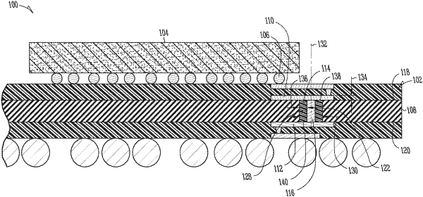
1. An electronic circuit comprising:
a substrate having a first side and a second side, the substrate including a first dielectric characteristic, the substrate further including a hole transverse to the first side, the hole extending from the first side to the second side;
a material disposed within the hole, the material including a second dielectric characteristic, wherein the second dielectric characteristic is different than the first dielectric characteristic;
a first conductive layer disposed on the first side and a second conductive layer disposed on the second side; and
a conductive path electrically coupled between the first conductive layer and the second conductive layer, wherein the conductive path is in contact with at least a portion of the material and traverses through the hole.
|