| CPC G11C 29/4401 (2013.01) [G11C 29/12015 (2013.01); H03K 5/1565 (2013.01); H03K 5/15066 (2013.01); H03K 19/1774 (2013.01); H03K 19/20 (2013.01)] | 20 Claims |

|
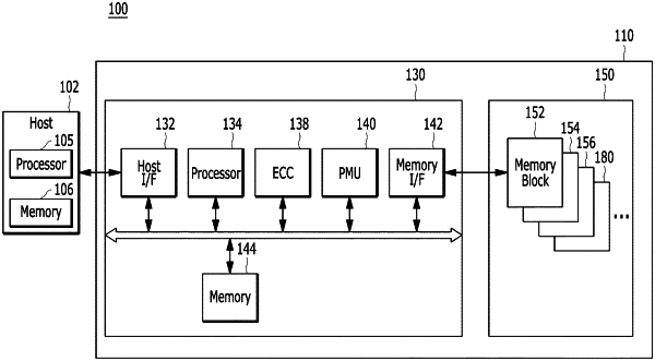
1. A memory system comprising:
a memory device including a plurality of memory blocks and a primary pulse correction module; and
a controller configured to transmit a control signal for controlling the memory device,
wherein the primary pulse correction module includes:
a reset signal generation circuit configured to generate a reset signal on the basis of the control signal;
a primary pulse detection circuit configured to output a detection signal by detecting a primary pulse of the control signal on the basis of the reset signal; and
a corrected primary pulse output circuit configured to correct a duty ratio of the primary pulse of the control signal to be outputted by adjusting a rising edge of the detection signal after the end of a preamble period of the control signal.
|