| CPC G11C 16/26 (2013.01) [G11C 7/08 (2013.01); G11C 8/14 (2013.01); G11C 16/0483 (2013.01); G11C 16/08 (2013.01); G11C 16/10 (2013.01); H10B 43/27 (2023.02); H10B 43/35 (2023.02); G11C 2207/2245 (2013.01)] | 7 Claims |

|
1. A semiconductor memory comprising:
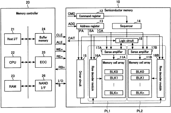
first to N-th memory cell arrays, N being an integer of 3 or more, an i-th memory cell array including a plurality of i-th memory cells, i being an integer from 1 to N; and
a controller, wherein
each of threshold voltages of the first to N-th memory cells is set to any of a first threshold voltage, a second threshold voltage higher than the first threshold voltage, a third threshold voltage higher than the second threshold voltage, and a fourth threshold voltage higher than the third threshold voltage,
data of six or more bits including a first bit, a second bit, a third bit, a fourth bit, a fifth bit, and a sixth bit is stored using a combination of a threshold voltage of the first memory cell, a threshold voltage of the second memory cell, and a threshold voltage of the third memory cell,
the controller is configured to perform a read operation for one bit data based on the first to N-th memory cell belonging to the first to N-th memory cell arrays, respectively, and
the controller applies first to N-th read voltages to the first to N-th memory cells, respectively, in parallel in the read operation.
|