| CPC G11C 16/24 (2013.01) [G11C 5/06 (2013.01); G11C 16/26 (2013.01); H10B 41/27 (2023.02); H10B 43/27 (2023.02)] | 20 Claims |

|
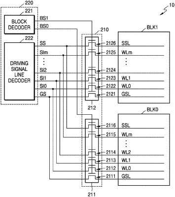
1. A memory device comprising:
a memory cell array including a first memory block and a second memory block adjacently disposed in a first direction;
driving signal lines respectively corresponding to vertically stacked word lines;
a first pass transistor circuit connected between the driving signal lines and the first memory block, the first pass transistor circuit including a first plurality of pass transistors controlled by a first block selection signal corresponding to the first memory block; and
a second pass transistor circuit connected between the driving signal lines and the second memory block, the second pass transistor circuit including a second plurality of pass transistors controlled by a second block selection signal corresponding to the second memory block,
wherein the first plurality of pass transistors and the second plurality of pass transistors are divided into an odd number of pass transistor groups disposed in the first direction,
wherein one of the odd number of pass transistor groups includes:
a first pass transistor connected between a first word line of the first memory block and a first driving signal line among the driving signal lines, and
a second pass transistor connected between a first word line of the second memory block and the first driving signal line, wherein the second pass transistor is adjacently disposed to the first pass transistor in a second direction.
|