US 11,837,273 B2
Semiconductor device having interconnection in package and method for manufacturing the same
Jaehyung Lee, Hwaseong-si (KR); JungSik Kim, Seoul (KR); Youngdae Lee, Yongin-si (KR); Duyeul Kim, Hwaseong-si (KR); Sungmin Yim, Suwon-si (KR); Kwangil Park, Yongin-si (KR); and Chulsung Park, Seoul (KR)
Assigned to SAMSUNG ELECTRONICS CO., LTD., Suwon-si (KR)
Filed by Samsung Electronics Co., Ltd., Suwon-si (KR)
Filed on Jul. 25, 2022, as Appl. No. 17/872,720.
Application 17/872,720 is a continuation of application No. 17/205,832, filed on Mar. 18, 2021, granted, now 11,417,386.
Application 17/205,832 is a continuation of application No. 16/734,821, filed on Jan. 6, 2020, granted, now 10,971,208, issued on Apr. 6, 2021.
Application 16/734,821 is a continuation of application No. 16/527,415, filed on Jul. 31, 2019, granted, now 11,328,760, issued on May 10, 2022.
Application 16/527,415 is a continuation of application No. 15/640,854, filed on Jul. 3, 2017, granted, now 10,418,087, issued on Sep. 17, 2019.
Application 15/640,854 is a continuation of application No. 14/697,634, filed on Apr. 28, 2015, granted, now 9,805,769, issued on Oct. 31, 2017.
Claims priority of application No. 10-2014-0086185 (KR), filed on Jul. 9, 2014.
Prior Publication US 2022/0358987 A1, Nov. 10, 2022
Int. Cl. G11C 11/4072 (2006.01); H01L 25/065 (2023.01); G11C 11/408 (2006.01); G11C 11/409 (2006.01); H01L 23/498 (2006.01); G11C 29/02 (2006.01); G11C 29/50 (2006.01); G11C 5/04 (2006.01); G11C 7/10 (2006.01)
CPC G11C 11/4072 (2013.01) [G11C 5/04 (2013.01); G11C 11/408 (2013.01); G11C 11/409 (2013.01); G11C 29/022 (2013.01); G11C 29/028 (2013.01); G11C 29/50008 (2013.01); H01L 23/49838 (2013.01); H01L 25/0655 (2013.01); G11C 7/109 (2013.01); G11C 7/1063 (2013.01); G11C 7/1075 (2013.01); H01L 2924/0002 (2013.01)] 20 Claims
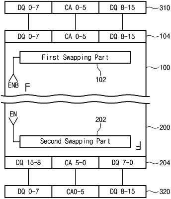
OG exemplary drawing
 
1. A multi-channel package comprising:
a package substrate;
a first die disposed on the package substrate and connected to a first channel, the first die including a plurality of first die data pads arranged in a first order;
a second die disposed on the package substrate and connected to a second channel, the second die being rotated 180 degrees with respect to the first die and including a plurality of second die data pads arranged in a second order;
a third die disposed on the package substrate and connected to a third channel; and
a fourth die disposed on the package substrate and connected to a fourth channel, the fourth die being rotated 180 degrees with respect to the third die,
wherein the second order is in reverse order from the first order,
wherein the first die and the second die are connected to each other through a first interconnection circuit, and
wherein the third die and the fourth die are connected to each other through a second interconnection circuit.