| CPC G09G 3/3266 (2013.01) [H10K 59/38 (2023.02); H10K 59/88 (2023.02); G09G 2300/0842 (2013.01); G09G 2310/08 (2013.01); G09G 2320/0219 (2013.01)] | 20 Claims |

|
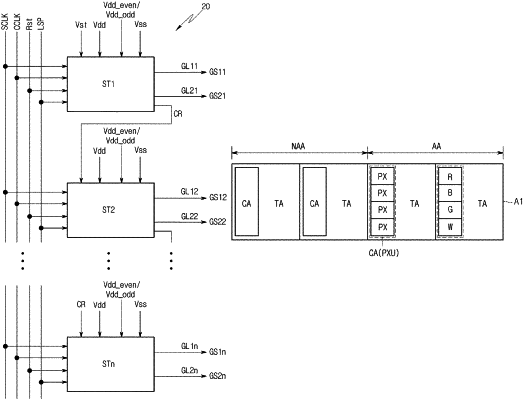
1. A gate driver, comprising:
a plurality of stages outputting gate signals to a plurality of gate lines respectively,
wherein each stage includes:
a plurality of circuit parts having circuit elements disposed thereon, the plurality of circuit parts spaced apart from each other; and
a plurality of transparent parts disposed between the plurality of circuit parts, the plurality of transparent parts permitting external light to pass through,
wherein the plurality of stages includes at least a first stage and a second stage,
wherein the first stage and the second stage each includes at least a first circuit part and a second circuit part,
wherein the first circuit part of the first stage and the first circuit part of the second stage are configured to perform the same function, and the second circuit part of the first stage and the second circuit part of the second stage are configured to perform the same function, and
wherein each of the plurality of circuit parts includes at least one circuit block required to perform a predetermined function of each of the plurality of circuit parts, and
wherein the plurality of circuit parts includes:
the first circuit part performing a function of controlling an output of a second gate signal provided to pixels for pixel sensing;
the second circuit part performing a function of setting a voltage of a first node disposed on the gate driver;
a third circuit part performing a function of controlling an output of a carry signal provided to another stage that is disposed after a corresponding stage;
a fourth circuit part performing a function of resetting the voltage of the first node and a voltage of a second node that is disposed on the gate driver, in response to the carry signal received from another stage that is disposed before the corresponding stage;
a fifth circuit part performing a function of inverting and outputting a signal applied to the first node and the second node;
a sixth circuit part performing a function of outputting a first gate signal at a gate-off voltage through at least one pull-down transistor that is turned on in response to the voltage of the second node; and
a seventh circuit part performing a function of outputting the first gate signal at a gate-on voltage through at least one pull-up transistor that is turned on in response to the voltage of the first node.
|