| CPC G09G 3/32 (2013.01) [G09G 2300/0443 (2013.01); G09G 2310/0267 (2013.01); G09G 2310/0275 (2013.01); G09G 2320/0233 (2013.01)] | 16 Claims |

|
1. A display panel, comprising:
a light emitting diode including an anode and a cathode; and
a pixel driving circuit which supplies a driving current to the light emitting diode,
wherein the anode is connected to a first power line to which a high potential voltage is supplied,
a sub pixel which includes the light emitting diode and the pixel driving circuit further includes:
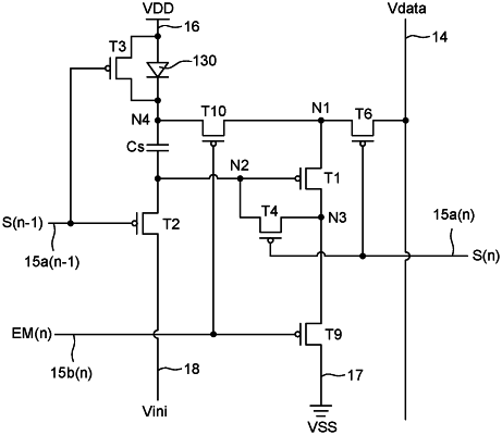
a driving element in which a source is connected to a N1 node, a gate is connected to a N2 node, and a drain is connected to a N3 node,
a switching circuit including a first electrode connected to the anode and the first power line, a second electrode connected to an n−1-th scan line or an n-th scan line, and a third electrode connected to the cathode;
a capacitor connected to the N2 node and a N4 node;
a N2 switching circuit connected to the N2 node;
a N3 switching circuit connected to the N3 node; and
a N1 switching circuit connected to the N1 node, and
wherein the N3 node is electrically connected to a second power line to which a low potential voltage is supplied,
wherein the third electrode is connected between the cathode and the N4 node or between the cathode and the N1 node, and
wherein the switching circuit is controlled by an n−1-th scan signal to supply high potential voltage to the N4 node or controlled by an n-th scan signal to supply high potential voltage to the N1 node.
|