US 11,836,347 B2
Memory system with selective access to first and second memories
Yasushi Nagadomi, Kanagawa (JP)
Assigned to KIOXIA CORPORATION, Tokyo (JP)
Filed by KIOXIA CORPORATION, Tokyo (JP)
Filed on Nov. 2, 2022, as Appl. No. 17/979,042.
Application 17/979,042 is a continuation of application No. 17/207,021, filed on Mar. 19, 2021, granted, now 11,494,077.
Application 17/207,021 is a continuation of application No. 16/671,674, filed on Nov. 1, 2019, granted, now 10,956,039, issued on Mar. 23, 2021.
Application 16/671,674 is a continuation of application No. 15/865,881, filed on Jan. 9, 2018, granted, now 10,474,360, issued on Nov. 12, 2019.
Application 15/865,881 is a continuation of application No. 15/012,549, filed on Feb. 1, 2016, abandoned.
Application 15/012,549 is a continuation of application No. 14/335,361, filed on Jul. 18, 2014, granted, now 9,280,461, issued on Mar. 8, 2016.
Application 14/335,361 is a continuation of application No. 14/063,278, filed on Oct. 25, 2013, granted, now 8,832,362, issued on Sep. 9, 2014.
Application 14/063,278 is a continuation of application No. 12/435,671, filed on May 5, 2009, granted, now 8,595,410, issued on Nov. 26, 2013.
Claims priority of application No. 2008-162281 (JP), filed on Jun. 20, 2008.
Prior Publication US 2023/0049754 A1, Feb. 16, 2023
This patent is subject to a terminal disclaimer.
Int. Cl. G06F 3/06 (2006.01); G06F 13/16 (2006.01); G06F 12/02 (2006.01); G06F 13/40 (2006.01)
CPC G06F 3/0604 (2013.01) [G06F 3/0629 (2013.01); G06F 3/0688 (2013.01); G06F 12/0246 (2013.01); G06F 13/1684 (2013.01); G06F 13/4022 (2013.01); G06F 2212/7202 (2013.01)] 11 Claims
OG exemplary drawing
 
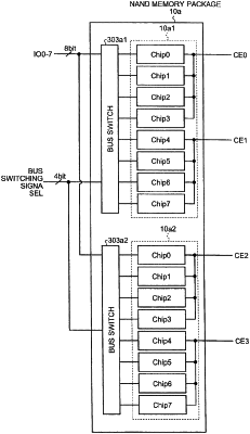
1. A memory device comprising:
a plurality of memory chips including at least a first memory chip;
a first signal line configured to receive a first signal, the first signal including IO data;
a second signal line configured to receive a first enable signal, the first enable signal selecting first target memory chips among the plurality of memory chips; and
a third signal line configured to receive a second enable signal different from the first enable signal, the second enable signal selecting second target memory chips among the plurality of memory chips; wherein
in a case where the first memory chip is included in both of the first target memory chips and the second target memory chips, the first memory chip is enabled to be accessed by the first signal.