| CPC G06F 12/0246 (2013.01) [G06F 3/06 (2013.01); G06F 3/061 (2013.01); G06F 3/0607 (2013.01); G06F 3/067 (2013.01); G06F 3/0658 (2013.01); G06F 3/0659 (2013.01); G06F 3/0664 (2013.01); G06F 3/0679 (2013.01); G06F 13/385 (2013.01); G06K 19/07732 (2013.01); G06K 19/07733 (2013.01); G06K 19/07749 (2013.01); H04B 1/3827 (2013.01); H04M 1/72412 (2021.01); G06F 2213/3804 (2013.01); G06F 2213/3814 (2013.01); H04M 1/0254 (2013.01); H04W 12/47 (2021.01)] | 16 Claims |

|
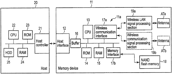
1. A memory system being connectable to a host device and an external device other than the host device, the system comprising:
a host interface to connect to the host device;
a wireless network interface to connect to the external device;
a nonvolatile memory which can store data from the host device and the external device;
a controller which controls the nonvolatile memory to write and read data in response to a request from the host device via the host interface;
a wireless communication module configured to transmit data stored in the nonvolatile memory to the external device or to receive data from the external device via the wireless network interface with a wireless communication; and
a register including a plurality of pages,
wherein the controller processes a first command to read data from the register, and processes a second command to write data to the register,
wherein a specific page of the register stores information indicating a number of one or more functions,
wherein the register includes a first address region to which a first function of the wireless communication is assigned and a second address region to which a second function of the wireless communication is assigned, the first address region and the second address region being located at different pages of the register, and
wherein the register further includes a first data port associated with the first function and a second data port associated with the second function.
|