| CPC G02F 1/134363 (2013.01) [G02F 1/1368 (2013.01); G02F 1/13439 (2013.01); G02F 1/133345 (2013.01); G02F 1/133512 (2013.01); G02F 1/134345 (2021.01); G02F 1/134372 (2021.01); G02F 2201/40 (2013.01)] | 9 Claims |

|
1. A liquid crystal device, comprising:
a first substrate and a second substrate that are disposed to face each other, the first substrate including a plurality of data lines and a plurality of scan lines intersecting the data lines;
a liquid crystal layer that is sandwiched between the first substrate and the second substrate;
a first electrode that is provided on a liquid crystal layer side of the first substrate;
an insulating layer that is provided on the liquid crystal layer side of the first electrode; and
a second electrode that is provided on the liquid crystal layer side of the insulating layer,
wherein:
sub-pixels are formed at regions surrounded by the data lines and the scan lines;
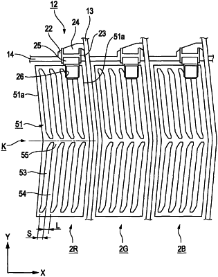
the second electrode has a plurality of gaps and a plurality of linear electrodes;
the gaps have a first bent portion, a second bent portion, a third bent portion, a fourth bent portion, a first linear portion, and a second linear portion, and the gaps include a first gap and a second gap, the first gap having the first bent portion, the third bent portion, and the first linear portion, and the second gap having the second bent portion, the fourth bent portion, and the second linear portion;
the first bent portion is connected to one end of the first linear portion, the third bent portion is connected to an other end of the first linear portion, the second bent portion is connected to one end of the second linear portion, the fourth bent portion is connected to an other end of the second linear portion,
the first bent portion and the third bent portion are inclined with respect to the first linear portion and are substantially parallel with each other,
the second bent portion and the fourth bent portion are inclined with respect to the second linear portion and are substantially parallel with each other,
the first bent portion faces the second bent portion at a substantially central portion of each of the sub-pixels in a long-axis direction of the sub-pixel,
the first linear portion extends from the first bent portion in a first direction,
the second linear portion extends from the second bent portion in a second direction different from the first direction, and
the entirety of each gap is bordered by material of the second electrode.
|