| CPC G02F 1/133345 (2013.01) [G02F 1/13394 (2013.01); G02F 1/13454 (2013.01); G02F 1/136286 (2013.01); G02F 1/1368 (2013.01); G02F 1/136227 (2013.01); G09G 3/3677 (2013.01); G09G 2300/0809 (2013.01)] | 19 Claims |

|
1. A display panel comprising:
a first display substrate including a display area and a non-display area disposed outside the display area;
a second display substrate facing the first display substrate; and
a sealant overlapping the non-display area and coupling the first display substrate and the second display substrate,
wherein:
the first display substrate comprises:
a plurality of insulating layers;
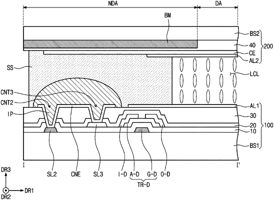
a first driving circuit overlapping the non-display area and comprising a connection electrode disposed on the insulating layers, a plurality of signal lines, and a plurality of second circuits connected to the signal lines;
a plurality of first lines overlapping the display area and connected to the first driving circuit;
a plurality of pixel transistors overlapping the display area and connected to the first lines;
a plurality of pixel electrodes disposed on the insulating layers and connected to the pixel transistors; and
an insulating pattern disposed on the insulating layers, covering the connection electrode, and making contact with the sealant;
the second circuits are arranged in a first direction; and
the first lines are respectively connected to the second circuits.
|