| CPC C23C 14/541 (2013.01) [C23C 14/0057 (2013.01); G11B 5/851 (2013.01); H10B 61/00 (2023.02); H10N 50/01 (2023.02)] | 7 Claims |

|
1. A method of fabricating a magnetic memory device, the method comprising:
forming a first magnetic metal layer on a substrate;
forming a non-magnetic metal oxide layer on the first magnetic metal layer using a first sputtering process to keep the substrate at or above a room temperature; and
forming a second magnetic metal layer on the non-magnetic metal oxide layer using a second sputtering process to cool the substrate to a temperature of 50K or less,
wherein the first sputtering process uses a first inert gas having a first evaporation point and the second sputtering process uses a second inert gas having a second evaporation point lower than the first evaporation point,
wherein the first inert gas is provided in a chamber, and
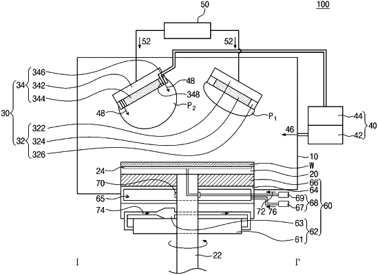
wherein the second sputtering process uses at least one of a plurality of sputter guns having a nozzle hole configured to spray the second inert gas in the chamber.
|