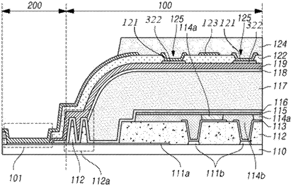
| CPC H10K 59/40 (2023.02) [G06F 3/0412 (2013.01); G06F 3/0416 (2013.01); G06F 3/0445 (2019.05); G06F 3/0446 (2019.05); H10K 50/844 (2023.02); H10K 59/131 (2023.02); G06F 2203/04103 (2013.01); G06F 2203/04111 (2013.01); G06F 2203/04112 (2013.01); H10K 59/1201 (2023.02); H10K 71/00 (2023.02)] | 22 Claims |

|
1. A display device comprising:
a substrate including a display area and a pad area;
a thin film transistor in the display area, and including a source electrode and a drain electrode;
a light emitting film layer including an anode electrode connected to the drain electrode, an organic light emitting film on the anode electrode, and a cathode electrode on the organic light emitting film;
an encapsulation layer including a first inorganic film, a first organic film on the first inorganic film, and a second inorganic film on the first organic film;
a touch buffer layer on the second inorganic film of the encapsulation layer;
a first bridge, a second bridge, a plurality of first touch electrodes and a plurality of second touch electrodes disposed on the touch buffer layer;
a touch insulating film disposed between the first bridge connecting the plurality of first touch electrodes and the second bridge connecting the plurality of second touch electrodes;
a touch pad in the pad area, and including an upper pad electrode and a lower pad electrode;
a touch sensing line connected to the plurality of first touch electrodes;
a touch driving line connected to the plurality of second touch electrodes; and
a signal line extending from the touch pad in the pad area to the display area,
wherein the signal line is interposed between the first inorganic film of the encapsulation layer and the substrate in the display area,
wherein at least one of the touch sensing line and the touch driving line is provided on a side surface of the encapsulation layer,
wherein both of the touch buffer layer and the touch insulating film are disposed between the at least one of the touch sensing line and the touch driving line and the side surface of the encapsulation layer in a sectional view,
wherein the first organic film of the encapsulation layer overlaps the at least one of the touch sensing line and the touch driving line provided on the side surface of the encapsulation layer,
wherein the touch driving line is in contact with the signal line exposed in the pad area to cause a signal to be conveyed to the plurality of second touch electrodes through the signal line,
wherein the first inorganic film and the second inorganic film extend toward an end of the display area, and the first inorganic film extends beyond an end of the second inorganic film toward the pad area,
wherein the touch buffer layer covers a side portion of the first inorganic film and directly contacts the side portion of the first inorganic film, and
wherein an end portion of at least a part of the touch buffer layer directly contacts both the upper pad electrode and the lower pad electrode where the upper pad electrode directly contacts the lower pad electrode.
|