| CPC H10K 59/131 (2023.02) [G09G 3/3258 (2013.01); H10K 59/1213 (2023.02)] | 20 Claims |

|
1. A display device comprising:
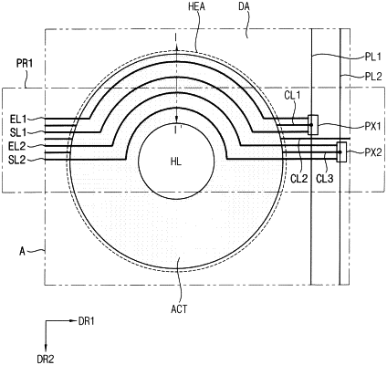
a substrate including a display area and a hole edge area, the display area surrounding the hole edge area, and the hole edge area defining a hole therein and surrounding the hole;
a plurality of pixels disposed in the display area in a first direction and a second direction intersecting the first direction;
an emission control line extending in the first direction in the display area, and bypassing the hole along the hole edge area;
a scan line extending in the first direction in the display area, located in the second direction apart from the emission control line, and bypassing the hole along the hole edge area;
an active pattern disposed in the hole edge area and not in the hole, overlapping the emission control line and the scan line in a plan view; and surrounding an entirety of the hole in the plan view; and
a connection line connected to the active pattern to provide a driving voltage to the active pattern,
wherein the hole is defined by an area in the hole edge area, and the area corresponds to removal of the substrate in the hole edge area defining a through-hole in the substrate, and
the active pattern is disposed between the substrate and the emission control line.
|