| CPC H04N 25/59 (2023.01) [H01L 27/14643 (2013.01); H01L 27/14656 (2013.01); H04N 25/575 (2023.01); H04N 25/589 (2023.01); H04N 25/622 (2023.01); H04N 25/75 (2023.01); H04N 25/76 (2023.01); H04N 25/771 (2023.01)] | 30 Claims |

|
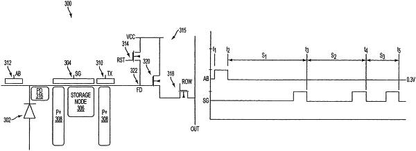
1. A pixel circuit, comprising:
a floating diffusion region;
a first photosensor coupled to the floating diffusion region via a first series of transistors;
a first storage region coupled to the first photosensor, the first storage region positioned between a first transistor and a second transistor of the first series of transistors;
a third transistor coupled to the first photosensor and separate from the first series of transistors, wherein the third transistor is configured such that the first photosensor is reset at least when the third transistor is activated while the first transistor is off;
a second photosensor coupled to the floating diffusion region via a second series of transistors different from the first series of transistors; and
a second storage region coupled to the second photosensor, the second storage region positioned between a fourth transistor and a fifth transistor of the second series of transistors, wherein the pixel circuit is configured to pulse a first signal applied to a gate of the third transistor such that (a) the third transistor is activated and the first photosensor is reset and (b) the pulse of the first signal ends before a second signal applied to a gate of the first transistor is asserted.
|