| CPC H04L 45/121 (2013.01) [H04L 49/9057 (2013.01); H04L 69/28 (2013.01)] | 21 Claims |

|
1. A reach-extension integrated circuit (IC) comprising:
first interface circuitry to receive a stream of logical blocks from a source external to the IC component, each of the logical blocks constituted by a respective set of symbols;
second interface circuitry to transmit the stream of logical blocks to a destination external to the IC component;
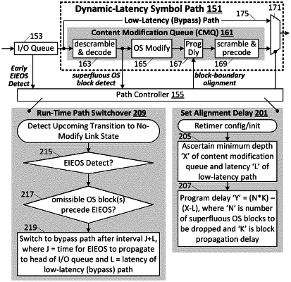
a first propagation path that, when enabled, shifts the stream of logical blocks from the first interface circuitry to the second interface circuitry with a first latency;
a second propagation path that, when enabled, shifts the stream of logical blocks from the first interface circuitry to the second interface circuitry with a second latency, the second propagation path including a variable delay circuit to enable the second latency to be adjusted such that a nonzero difference between the first latency and the second latency corresponds to a time required for an integer number of the logical blocks to propagate into the second propagation path from the first interface circuitry; and
path control circuitry to effect, by enabling the first propagation path and disabling the second propagation path, a switchover from the second propagation path to the first propagation path that occurs, due to the adjustment of the second latency via the variable delay circuit, at a boundary between successive logical blocks within the stream of logical blocks.
|