| CPC H02J 50/402 (2020.01) [H02J 50/10 (2016.02); H02J 50/60 (2016.02); H02J 50/70 (2016.02)] | 16 Claims |

|
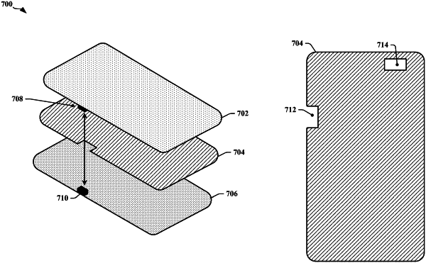
1. A wireless charging device, comprising:
a first printed circuit board having a first surface with a first plurality of charging cells formed thereon;
a second printed circuit board having a first surface with a second plurality of charging cells formed thereon;
a third printed circuit board having an opening formed therein;
one or more fastenings configured to align and fasten the first printed circuit board to and the second printed circuit board when the third printed circuit board is located between the first printed circuit board and the second printed circuit board; and
a connector configured to electrically couple the first printed circuit board to the second printed circuit board when the first printed circuit board and the second printed circuit board are fastened and aligned,
wherein the connector is further configured to pass through the opening in the third printed circuit board, and
wherein a charging surface of the wireless charging device is provided using the first plurality of charging cells and the second plurality of charging cells when the first printed circuit board and the second printed circuit board are fastened and aligned.
|