| CPC H01R 13/03 (2013.01) [H01B 5/02 (2013.01); H01B 7/0045 (2013.01); H01R 12/58 (2013.01); H01R 13/502 (2013.01); H01R 43/16 (2013.01)] | 18 Claims |

|
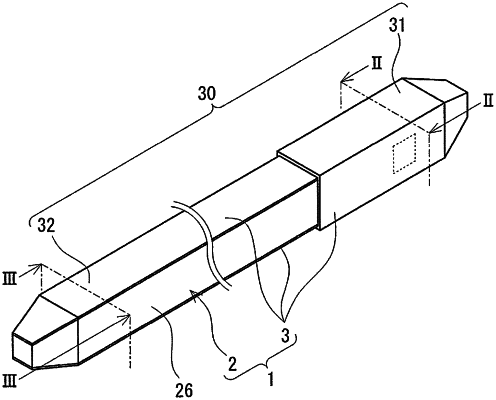
1. A pin terminal, comprising:
a bar-like base material; and
a plating layer covering a predetermined region of the base material,
wherein:
a constituent material of the base material is pure copper or a copper alloy,
the plating layer includes a tin-based layer made of metal containing tin,
one end side of the base material includes a tip covering portion,
the tin-based layer includes the tip covering portion,
the tip covering portion covers an entire region in a circumferential direction on the one end side of the base material, and
a difference (t1−t2) between a maximum value t1 and a minimum value t2 of a thickness of the tip covering portion measured at a measurement location set at a spot of 1 mm from one end of the pin terminal along a longitudinal direction of the pin terminal is 0.20 μm or more.
|