| CPC H01L 29/78606 (2013.01) [H01L 21/0217 (2013.01); H01L 21/02274 (2013.01); H01L 21/02565 (2013.01); H01L 27/1225 (2013.01); H01L 27/127 (2013.01); H01L 29/66969 (2013.01); H01L 29/78633 (2013.01); H01L 29/78648 (2013.01); H01L 29/7869 (2013.01); H10K 59/1213 (2023.02)] | 12 Claims |

|
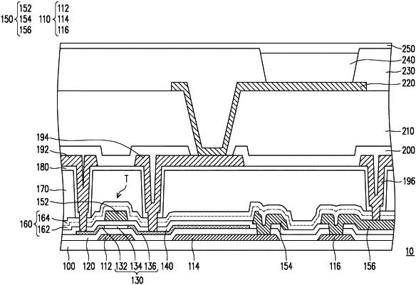
1. An active device substrate, comprising:
a substrate;
an active device, located on the substrate, wherein the active device comprises:
a semiconductor layer, located on the substrate;
a first gate overlapping with and located on the semiconductor layer;
a gate insulation layer sandwiched between the first gate and the semiconductor layer; and
a source and a drain, electrically connected to the semiconductor layer; and
a barrier layer comprising:
a first hydrogen atom distribution region, located on the active device, wherein the first hydrogen atom distribution region comprises silicon nitride and hydrogen atoms, wherein the first hydrogen atom distribution region contacts and covers a portion of a top surface of the gate insulation layer, wherein the first hydrogen atom distribution region contacts and covers a top surface and a side surface of the first gate; and
a second hydrogen atom distribution region, wherein the first hydrogen atom distribution region is located between the second hydrogen atom distribution region and the semiconductor layer, wherein the second hydrogen atom distribution region includes silicon nitride and hydrogen atoms, wherein the concentration of nitrogen atoms in the first hydrogen atom distribution region is smaller than the concentration of nitrogen atoms in the second hydrogen atom distribution region, and the highest concentration of the hydrogen atoms in the first hydrogen atom distribution region is greater than the highest concentration of the hydrogen atoms in the second hydrogen atom distribution region, wherein the thickness of the first hydrogen atom distribution region is less than or equal to the thickness of the second hydrogen atom distribution region.
|