| CPC H01L 29/66545 (2013.01) [H01L 21/02532 (2013.01); H01L 21/02636 (2013.01); H01L 21/0337 (2013.01); H01L 21/28247 (2013.01); H01L 21/28518 (2013.01); H01L 21/28568 (2013.01); H01L 21/3086 (2013.01); H01L 21/31105 (2013.01); H01L 21/31144 (2013.01); H01L 21/76224 (2013.01); H01L 21/76232 (2013.01); H01L 21/76801 (2013.01); H01L 21/76802 (2013.01); H01L 21/76816 (2013.01); H01L 21/76834 (2013.01); H01L 21/76846 (2013.01); H01L 21/76849 (2013.01); H01L 21/76877 (2013.01); H01L 21/76897 (2013.01); H01L 21/823431 (2013.01); H01L 21/823481 (2013.01); H01L 21/823807 (2013.01); H01L 21/823814 (2013.01); H01L 21/823821 (2013.01); H01L 21/823828 (2013.01); H01L 21/823842 (2013.01); H01L 21/823857 (2013.01); H01L 21/823871 (2013.01); H01L 21/823878 (2013.01); H01L 23/5226 (2013.01); H01L 23/528 (2013.01); H01L 23/5283 (2013.01); H01L 23/53209 (2013.01); H01L 23/53238 (2013.01); H01L 23/53266 (2013.01); H01L 23/5329 (2013.01); H01L 27/0207 (2013.01); H01L 27/0886 (2013.01); H01L 27/0922 (2013.01); H01L 27/0924 (2013.01); H01L 28/20 (2013.01); H01L 28/24 (2013.01); H01L 29/0649 (2013.01); H01L 29/0653 (2013.01); H01L 29/0847 (2013.01); H01L 29/165 (2013.01); H01L 29/167 (2013.01); H01L 29/41783 (2013.01); H01L 29/41791 (2013.01); H01L 29/516 (2013.01); H01L 29/6653 (2013.01); H01L 29/6656 (2013.01); H01L 29/66636 (2013.01); H01L 29/66795 (2013.01); H01L 29/66818 (2013.01); H01L 29/7843 (2013.01); H01L 29/7845 (2013.01); H01L 29/7846 (2013.01); H01L 29/7848 (2013.01); H01L 29/785 (2013.01); H01L 29/7851 (2013.01); H01L 29/7854 (2013.01); H10B 10/12 (2023.02); H01L 21/02164 (2013.01); H01L 21/0217 (2013.01); H01L 21/0332 (2013.01); H01L 21/76883 (2013.01); H01L 21/76885 (2013.01); H01L 21/823437 (2013.01); H01L 21/823475 (2013.01); H01L 24/16 (2013.01); H01L 24/32 (2013.01); H01L 24/73 (2013.01); H01L 29/665 (2013.01); H01L 29/7842 (2013.01); H01L 29/7853 (2013.01); H01L 2224/16227 (2013.01); H01L 2224/32225 (2013.01); H01L 2224/73204 (2013.01)] | 21 Claims |

|
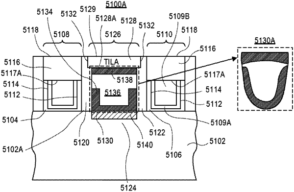
1. An integrated circuit structure, comprising:
a three-dimensional body comprising silicon;
a gate electrode completely surrounding a channel region of the three-dimensional body, the gate electrode having a first side and a second side opposite the first side,
a gate insulating cap on the gate electrode, the gate insulating cap having a top surface and a bottom surface;
a dielectric spacer adjacent the first side of the gate electrode and adjacent the gate insulating cap;
a semiconductor source or drain region adjacent the dielectric spacer;
a trench contact structure over the semiconductor source or drain region, the trench contact structure comprising an insulating cap on a conductive structure, the insulating cap of the trench contact structure having a top surface substantially co-planar with the top surface of the gate insulating cap, and the insulating cap of the trench contact structure having a bottom surface above the bottom surface of the gate insulating cap.
|