| CPC H01L 29/66439 (2013.01) [H01L 29/0603 (2013.01); H01L 29/15 (2013.01); H01L 29/41741 (2013.01); H01L 29/42392 (2013.01)] | 20 Claims |

|
1. A method for making a semiconductor device comprising:
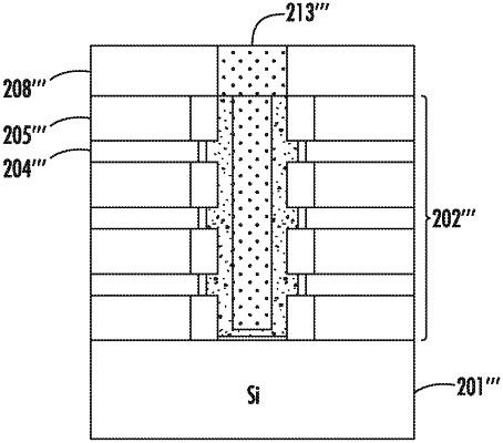
forming a plurality of spaced apart gate stacks on a substrate defining respective trenches therebetween, each gate stack comprising alternating layers of first and second semiconductor materials, the layers of the second semiconductor material defining nanostructures;
forming respective source/drain regions within the trenches;
forming respective insulating regions adjacent lateral ends of the layers of the first semiconductor material; and
forming respective dopant blocking superlattices adjacent lateral ends of the nanostructures and offset outwardly from adjacent surfaces of the insulating regions, each dopant blocking superlattice comprising a plurality of stacked groups of layers, each group of layers comprising a plurality of stacked base semiconductor monolayers defining a base semiconductor portion, and at least one non-semiconductor monolayer constrained within a crystal lattice of adjacent base semiconductor portions.
|