| CPC H01L 27/14636 (2013.01) [H01L 24/09 (2013.01); H01L 24/70 (2013.01); H01L 27/14601 (2013.01); H01L 27/14634 (2013.01); H01L 27/14643 (2013.01); H04N 25/63 (2023.01)] | 23 Claims |

|
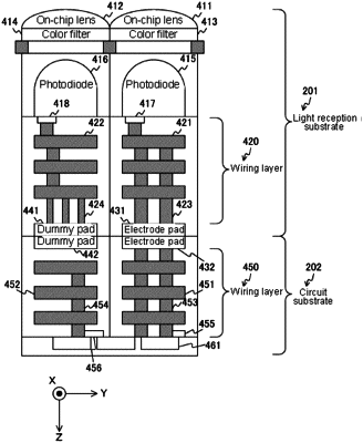
1. An image sensor, comprising:
a first substrate including a plurality of pixels and a plurality of vertical signal lines and a plurality of first wiring layers at one side thereof;
a second substrate including a plurality of second wiring layers at one side thereof,
wherein the first and second substrates are secured together between the pluralities of first and second wiring layers;
first pads provided between one of the plurality of first wiring layers and one of the plurality of second wiring layers;
second pads provided between another of the plurality of first wiring layers and another of the plurality of second wiring layers;
first vias connecting the one of the plurality of first wiring layers and the first pad provided on the first substrate;
second vias connecting the one of the plurality of second wiring layers and the first pad provided on the second substrate,
wherein the first pad provided on the first substrate and the second pad provided on the second substrate are connected to each other;
third vias connecting the another of the plurality of first wiring layers; and
fourth vias connecting the another of the plurality of second wiring layers,
wherein at least one of the third vias and the fourth vias connect the second pads and at least one of the another of the plurality of first and second wiring layers together,
wherein the first pads provide for electrical connection between the one of the plurality of first wiring layers and the one of the plurality of second wiring layers and the first pads are electrically connected to one of the plurality of vertical signal lines, and
wherein the second pads do not electrically connect to the plurality of vertical signal line.
|