| CPC H01L 27/14621 (2013.01) [H01L 27/14607 (2013.01); H01L 27/14625 (2013.01); H01L 27/14645 (2013.01); H04N 25/75 (2023.01); H04N 25/77 (2023.01)] | 14 Claims |

|
1. A sensing device, comprising:
a light-emitting panel adapted to emit an initial light with a first waveform; and
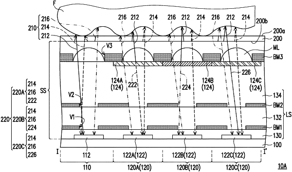
a sensing pixel array structure located on a back side of the light-emitting panel, wherein the sensing pixel array structure comprises:
a plurality of first sensing pixel structures, wherein each of the first sensing pixel structures comprises a first sensing element, and the initial light with the first waveform reflected by a to-be sensed object is served as a first sensing light received by the first sensing element for sensing;
at least one second sensing pixel structure, wherein the at least one second sensing pixel structure comprises a second sensing element and a light conversion layer, the light conversion layer is located between the second sensing element and the light-emitting panel, the light conversion layer has an excitation peak wavelength and the excitation peak wavelength is in a range of 400 nm to 750 nm, and the light conversion layer of the at least one second sensing pixel structure is adapted to convert the initial light with the first waveform reflected by a to-be sensed object to a second sensing light received by the second sensing element for sensing, and the second sensing light has a second waveform different from the first waveform; and
at least one third sensing pixel structure, wherein the at least one third sensing pixel structure comprises a third sensing element and a color filter layer, the color filter layer is located between the third sensing element and the light-emitting panel, the color filter layer has filter characteristics to shield and/or absorb light in a specific wavelength range while only allowing light in another specific wavelength range to pass, the color filter layer of the at least one third sensing pixel structure is adapted to adjust the initial light with the first waveform to a third sensing light to be provided to the third sensing element for sensing, and the third sensing light has a third waveform different from the first waveform and the second waveform,
wherein the second sensing light comprises a converted light obtained by the light conversion layer converting a portion of the reflected initial light with the first waveform and another portion of the reflected initial light with the first waveform, the first waveform of the reflected initial light comprises a first wavelength portion and a second wavelength portion in a longer wavelength range than the first wavelength portion, the converted light comprises a converted wavelength portion converted from the first wavelength portion of the reflected initial light with the first waveform, and the converted wavelength portion is in a wavelength range overlapping the second wavelength portion.
|