| CPC H01L 27/14603 (2013.01) [G09G 3/3648 (2013.01); H01L 27/14612 (2013.01); H01L 27/14616 (2013.01); H01L 27/14625 (2013.01); H01L 27/14636 (2013.01); H01L 27/14641 (2013.01); H01L 27/14643 (2013.01); H01L 29/7869 (2013.01); G09G 2354/00 (2013.01)] | 13 Claims |

|
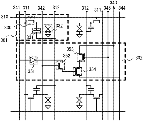
1. An electronic device comprising a pixel, the pixel comprising:
a photodiode;
a first wire electrically connected to an anode of the photodiode;
a second wire electrically connected to the first wire;
a first transistor;
a second transistor; and
a third transistor,
wherein a gate of the first transistor is electrically connected to a third wire,
wherein one of a source and a drain of the first transistor is electrically connected to a cathode of the photodiode,
wherein the other of the source and the drain of the first transistor is electrically connected to a fourth wire,
wherein a gate of the second transistor is electrically connected to the fourth wire,
wherein one of a source and a drain of the second transistor is electrically connected to a fifth wire,
wherein a gate of the third transistor is electrically connected to a sixth wire,
wherein one of a source and a drain of the third transistor is electrically connected to the other of the source and the drain of the second transistor,
wherein the other of the source and the drain of the third transistor is electrically connected to a seventh wire, and
wherein the first wire and the second wire are positioned in different layers.
|