| CPC H01L 24/05 (2013.01) [H01L 23/5226 (2013.01); H01L 24/03 (2013.01); H01L 24/13 (2013.01); H01L 23/53238 (2013.01); H01L 2224/05018 (2013.01); H01L 2224/05025 (2013.01); H01L 2224/05083 (2013.01); H01L 2224/05166 (2013.01); H01L 2224/05181 (2013.01); H01L 2224/05184 (2013.01); H01L 2224/05186 (2013.01); H01L 2224/05547 (2013.01); H01L 2224/05561 (2013.01); H01L 2224/05572 (2013.01); H01L 2224/05624 (2013.01); H01L 2224/05686 (2013.01); H01L 2224/13026 (2013.01)] | 12 Claims |

|
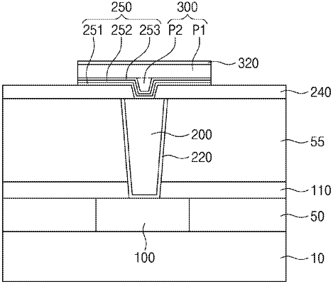
1. A semiconductor device, comprising:
a first dielectric layer on a lower structure including a substrate;
a first pad in the first dielectric layer;
a lower passivation layer on the first dielectric layer;
a second dielectric layer on the lower passivation layer;
a via hole penetrating the second dielectric layer and the lower passivation layer to expose the first pad;
a through electrode arranged within the via hole and electrically connected to the first pad in the via hole, wherein a top surface of the through electrode is at a same level as or a lower level than a top of the via hole;
an upper passivation layer having a recess region partially exposing the through electrode on the second dielectric layer;
an upper barrier layer conformally formed from a top surface of the upper passivation layer to an inner surface of the recess region; and
a second pad on the upper barrier layer,
wherein the second pad comprises:
an inner part surrounded by the upper barrier layer in the recess region;
an outer part on a top surface of the upper barrier layer and the inner part.
|