| CPC H01L 23/544 (2013.01) [H01L 21/56 (2013.01); H01L 23/18 (2013.01); H01L 23/3114 (2013.01); H01L 24/05 (2013.01); H01L 27/148 (2013.01); H01L 2223/54426 (2013.01); H01L 2224/0401 (2013.01); H01L 2224/04105 (2013.01); H01L 2224/05022 (2013.01); H01L 2924/181 (2013.01)] | 16 Claims |

|
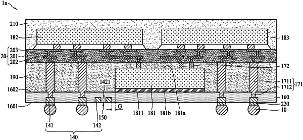
1. A semiconductor package structure, comprising:
a first passivation layer;
a first semiconductor die disposed over the first passivation layer;
a first metal layer adjacent to the first passivation layer, wherein the first metal layer includes a first portion and a second portion spaced apart from the first portion, and the first portion is geometrically distinct from the second portion from a top view perspective;
a second semiconductor die electrically connected to the first semiconductor die; and
a third semiconductor die electrically connected to the first semiconductor die,
wherein the second semiconductor die is electrically connected to the third semiconductor die through the first semiconductor die, wherein the first portion of the first metal layer is configured to serve as an alignment mark,
wherein the first portion is vertically overlapped with the second semiconductor die.
|