| CPC H01L 23/49503 (2013.01) [H01L 23/3107 (2013.01); H01L 23/49541 (2013.01); H01L 24/40 (2013.01); H01L 2224/40175 (2013.01)] | 12 Claims |

|
1. A semiconductor package comprising:
a lead frame comprising
a first die paddle; and
one or more leads disposed along a first side of the first die paddle;
a chip mounted on the first die paddle; and
a molding encapsulation enclosing the chip;
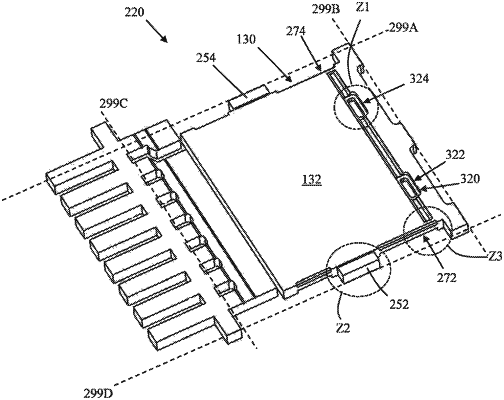
wherein the first die paddle comprises:
one or more through holes aligned in parallel and approximate to a second side of the first die paddle opposite the first side of the first die paddle;
a first protrusion extending beyond an edge of the first die paddle at a third side orthogonal to the first and second sides;
a second protrusion extending beyond an edge of the first die paddle at a fourth side opposite to the third side;
wherein an entirety of the one or more through holes is filled with a first portion of the molding encapsulation
wherein the first protrusion comprises:
a first groove substantially aligned to the edge of the first die paddle at the third side separating a top surface of the first protrusion from a top surface of the first die paddle;
wherein an entirety of the first groove is filled with a second portion of the molding encapsulation;
wherein the second protrusion comprises:
a second groove substantially aligned to the edge of the first die paddle at the fourth side separating a top surface of the second protrusion from the top surface of the first die paddle;
wherein the first protrusion and the second protrusion are symmetric with respect to a centerline of a bottom surface of the semiconductor package;
wherein a portion of the top surface of the first protrusion is exposed from the molding encapsulation; and
wherein a portion of the top surface of the second protrusion is exposed from the molding encapsulation.
|