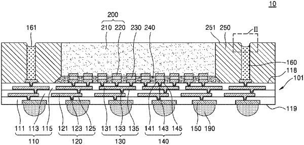
| CPC H01L 23/3114 (2013.01) [H01L 23/293 (2013.01); H01L 23/3121 (2013.01); H01L 23/5226 (2013.01)] | 20 Claims |

|
1. A semiconductor package comprising:
a semiconductor chip including a chip pad, the chip pad disposed on a lower surface of the semiconductor chip;
a lower redistribution structure on the lower surface of the semiconductor chip, the lower redistribution structure including a lower redistribution insulating layer and a lower redistribution pattern electrically connected to the chip pad of the semiconductor chip;
a molding layer on at least a portion of the semiconductor chip and on an upper surface of the lower redistribution structure; and
a conductive post in the molding layer, the conductive post having a bottom surface and a top surface, the bottom surface of the conductive post being in contact with the lower redistribution pattern of the lower redistribution structure and the top surface of the conductive post having a concave shape,
wherein the top surface of the conductive post is at a lower level than a top surface of the molding layer,
wherein the conductive post is on an inner wall of the molding layer, a first portion of the inner wall of the molding layer contacting a sidewall of the conductive post and a second portion of the inner wall of the molding layer being exposed and extending vertically above the top surface of the conductive post, wherein the first and second portions of the inner wall of the molding layer are vertically coplanar with each other and with the sidewall of the conductive post, and wherein a corner portion of the molding layer slopes downward from the top surface of the molding layer to the second portion of the inner wall of the molding layer.
|