| CPC H01L 21/823871 (2013.01) [H01L 21/02603 (2013.01); H01L 21/76805 (2013.01); H01L 21/76831 (2013.01); H01L 21/76895 (2013.01); H01L 21/76897 (2013.01); H01L 21/823807 (2013.01); H01L 21/823814 (2013.01); H01L 27/092 (2013.01); H01L 29/0673 (2013.01); H01L 29/0847 (2013.01); H01L 29/41733 (2013.01); H01L 29/42392 (2013.01); H01L 29/78618 (2013.01); H01L 29/78696 (2013.01)] | 20 Claims |

|
1. A semiconductor structure, the semiconductor structure comprising:
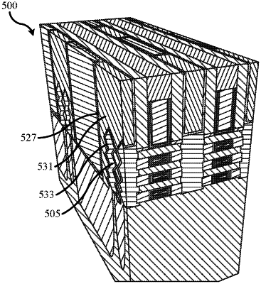
two contact regions proximate a gate and separated by an interior region proximate the gate, wherein a metal material is formed about contacts in the two contact regions, wherein the interior region comprises a liner material, the interior region comprises an oxide layer between the liner material and a spacer layer, and the spacer layer is between the oxide layer and the gate, and wherein the contacts comprise multiple sections of a sawtooth profile along both vertical sides of the contacts such that the metal material fills the multiple sections of the sawtooth profile around the contacts.
|
|
8. A semiconductor structure, the semiconductor structure comprising:
two contact regions proximate a gate and separated by an interior region proximate the gate, wherein a metal material is formed about contacts in the two contact regions, the contacts comprise multiple sections of a sawtooth profile along both vertical sides of the contacts such that the metal material fills the multiple sections of the sawtooth profile around the contacts, and the interior region comprises a liner material and an oxide contact etch stop layer between the two contact regions.
|
|
16. A semiconductor structure, the semiconductor structure comprising:
two contact regions proximate a gate and separated by an interior region proximate the gate, wherein a metal material is formed around contacts in the two contact regions down to a substrate, wherein the interior region comprises a liner material and an oxide layer between the two contact regions, and wherein the contacts comprise multiple sections of a sawtooth profile along both vertical sides of the contacts such that the metal material fills the multiple sections of the sawtooth profile around the contacts.
|